LITHOGRAPHY
Instead of using a light source, such as in optical lithography, electron beam (e-beam) lithography utilizes an electron beam to generate the patterns on the sample. Because of the much shorter wavelength, we can achieve much higher resolution features; however, because it is a single electron beam writing the sample, it takes longer to generate the pattern on the sample.
LITHOGRAPHY EQUIPMENT
E-BEAM Vistec
E-BEAM Raith
E-BEAM JEOL
MASK ALIGNER EVG620
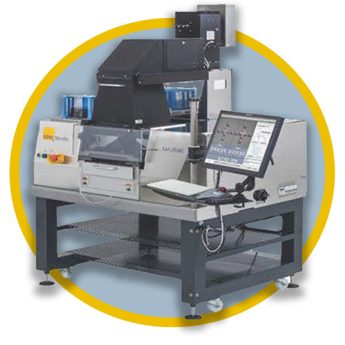
MASK ALIGNER+ NANOIMP.SUSS
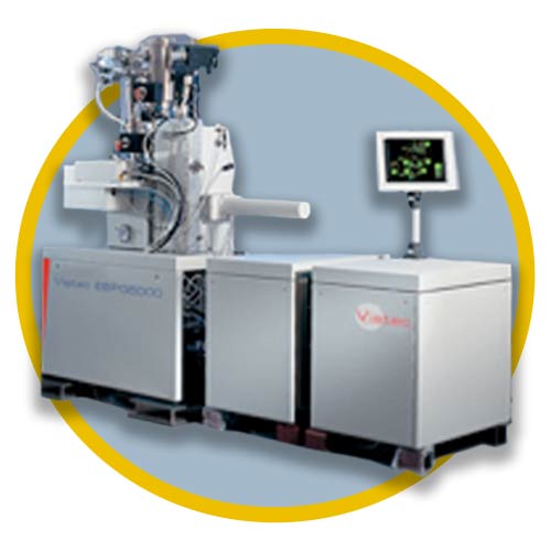
E-BEAM LITHOGRAPHY VISTEC-EBPG5000
The Vistec EBPG 5200 is a dedicated direct-write Electron Beam capable of patterning large areas by high-resolution. This instrument has substrate holders to handle 3″ wafers, piece parts from a couple of mm to 3″ diameter and 6″ mask plates. While this instrument can be set to operate at 20, 50, or 100 keV, it is normally set for 100 keV operation.
Type of EO system:
Gaussian Beam
Voltage:
50 and 100 KeV
Sean Freq:
10 MHz
Cassette Size:
Up to 6” wafers (150mm)
Field Size:
1 µm to 1 mm
Beam current:
100 pA … 300 nA
Spot size:
2 … >350 nm (defocussed)
Main field resolution:
0.16 … 1.0 nm
Main field size:
160 (167.77216) … 1000 (1048.576) μm (20 bit)
Subfield resolution:
0.08 … 0.5 nm
Subfield size:
1.31072 … 4.525 μm (14 bit, 100 kV)
Beam step size:
0.08 … 4096 nm
lnterferometer resolution:
0.154 nm (λ/4096)
In field distortion:
< 10 nm (mean+ 3s)
Stitching:
< 20 nm (mean+ 3s)
Alignment:
< 20 nm (mean+ 3s)
Operating system:
Red Hat Enterprise Linux
E-BEAM RAITH 150
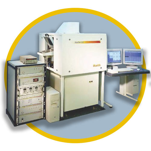
The Raith 150 is an electron beam capable of exposing structures smaller than 10 nm and working with sample sizes from a few mm to 6-inch wafers. Its filament works from 0.2 to 30 KeV and has a pattern generator of 20 MHz. With itsKV imaging capabilities, the Raith150 e-beam alsos allows for surface-sensitive high-resolution isnpection, metrology and process control.
Type of EO system:
Gaussian Beam
Voltage:
100 eV to 30 KeV TFE filament
Sean Freq:
20 MHz
Cassette Size:
150 mm {6″)
Field Size:
1 µm to 1 mm
Beam size 1 ke V using the 30 μm aperture:
4 nm
Beam size 20 ke V using the 30 μm aperture:
2 nm
Beam position drift: with resting stage, register 1 mark every 15 min, at 10 keV:
maximum 10 nm/min or 600 nm/hour
Lithography specifications Minimum feature size:
minimum feature size <20.0 nm
ELECTRON BEAM LITHOGRAPHY SUSTEM. JBX-8100FS
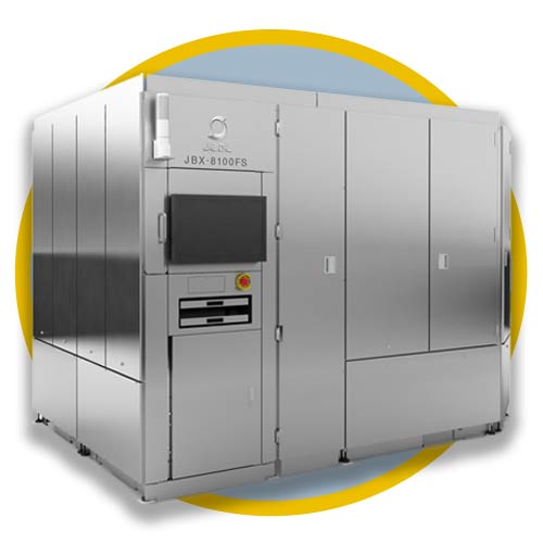
The JBX-8100FS writes ultrafine patterns (5nm) at a faster rate of speed while minimizing idle time, especially during the exposure process, thus increasing throughput. The system has substrate cassettes for few mm piece parts, 4-inch, 6-inch and 8-inch wafers as well as for 7-inch masks and includes an autoloader whith 12 positions. It includes two writing modes: High resolution (with writefiels of 100 microns) and High throughput mode (writefields of 1mm). It makes use of a100 KV Schottky FEG filament and has a pattern generator of 125 MHz.
Type of EO system:
Gaussian Beam
Voltage:
100kV Schottky FEG
Sean Freq:
125MHz
Cassette Size:
200mm (8″)
Field Size:
(HT mode) 1,000um x 1,000um
(HR mode) 100um x 100um
Stitching Accuracy:
+/- 20nm
+/- 20nm
8<snm
Overlay Accuracy:
0.62nm
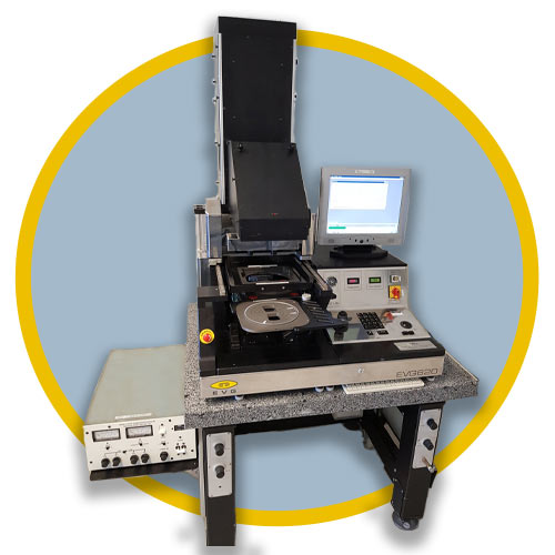
MASK ALIGNER EVG620
Wafer size:
4″ 6″
Exposure:
Proximity, Soft, Hard contact
Resolution:
<1,5µm (hard contact)
Lamp wavelength:
Mercury 365-465nm
Alignment accuracy:
±1µm
SUSS MA/BA8 Gen4 Mask Aligner & SMILE Imprint up to 200mm wafers
The MA/BA 8 is a combination mask aligner and NIL equipment (Nanoimprint Lithography). The mask aligner has a LED UV lamp which allows to make photolithography on 4”, 6” and 8” wafers with a 0.5 um precision alignment. The NIL offers a <50um resolution for nanoimprint on substrates up to 8” with a residual thickness layer below 25nm. It also has a separate unit (UV-SFT8) for the fabrication of stamps made on flexible foils..
Wafer size:
4″6″8″
Mask aligner:
Top side alignment (accuracy<0,5µm)
Lamp UV-LED (i-line,h-line,g-line)
Line/space resolution <0,8µm (6”)
/ <1,5µm (8″) (vacuum contact)
Nanoimprint SMILE:
UV-SFT8 (UV-LED) unit far stamp fabrication resolution <50nm
Residual layerthickness <25nm
