HOUSING
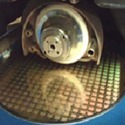
The marking and cutting process separates the chips that make up the processed wafer. Usually, the dicing process needs a machine called a dicing saw or laser cutting.

HOUSING EQUIPMENT
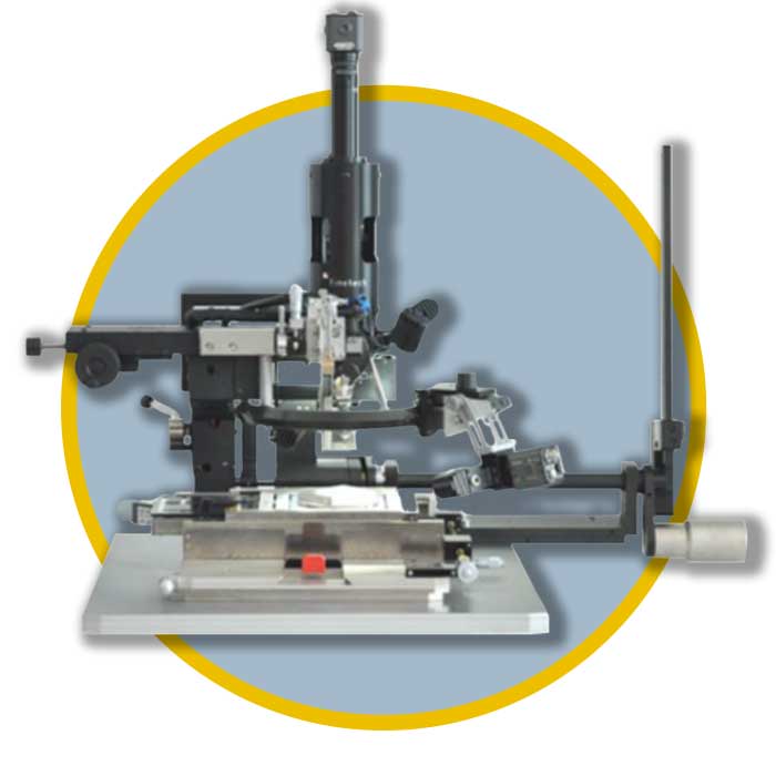
FINETECH FINEPLACER PICO MA
This versatile platform is used in a wide range of micro assembly applications such as flip chip bonding (face down), precise die bonding (face up), Laser diode, laser diode bar bonding Optical engines, VCSEL/photo diode bonding LED bonding Micro optics assembly MEMS/ MOEMS/ sensor packaging 3D packaging Wafer level packaging (W2W, C2W) Chip on glass, chip on flex.
Placement accuracy:
5 µm
Field of view (min):
1.6 mm x 1.2 mm
Field of view (max):
20 mm x 15 mm
Component size (min):
0.125 mm x 0.125 mm
Component size (max):
40 mm x 40 mm
Theta fine travel:
± 6°
Z- travel:
10 mm
Working area:
280 mm x 117 mm
Heating temp. (max):
1,2*: 400 °C
Bonding force (max):
1,2*: 700 N

