DIE-ATTACH
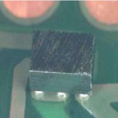
A process typically applied to mount devices such as semiconductor lasers or optical amplifiers onto substrates within a few microns of accuracy. Assembly requires a temperature cycle that causes the chip and base contacting surfaces to weld together.


FLIP-CHIP
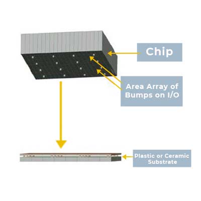
This connection technique is where small «balls» (bumps) of conductive material are deposited on each of the pads of the circuit. Then, the chip is placed inverted with the bumps coinciding with the pads of the circuit to be soldered (pad+bump+pin) simultaneously applying pressure and high temperature. The flip chip technique produces more close connections and a higher precision (± 0.5 μm).

DIE-ATTACH AND FLIP-CHIP EQUIPMENT
FC-150 AUTOMATED DEVIDE BONDER
FINEPLACER A4V PICO
FC-150 AUTOMATED DEVIDE BONDER
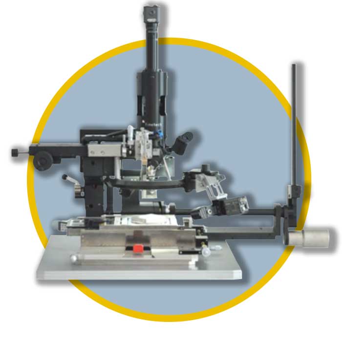
The S.E.T FC 150 is a precision instrument used to align and bond one or more chips on a substrate, using one of several available techniques (Z control using reflow or UV, thermo-compression, cold compression and compression together with UV glue curing). The FC 150 combines pre-programmed instructions for site location and bonding parameters together with user or pattern recognition software control for alignment.
Handling:
Chip Size: 0,2 – 40 mm
Substrate Size: 0.5 -150 mm
Main XY STAGE:
X Travel: 300 mm
Y Travel: 250 mm
Sensitivity: 1 µm
Flatness: ±2µm
High Resolution XY stage:
X Travel: 50µm
Y Travel 50µm
Sensitivity: 0,1 µm
Angle Z Chuck support:
Z Travel: 6 mm
Angle Travel: ±7 °
Z Sensitivity: 0.5 µm
Angle Sensitivity: 10-4 rad

FINETECH FINEPLACER PICO MA
This versatile platform is used in a wide range of micro assembly applications such as flip chip bonding (face down), precise die bonding (face up), Laser diode, laser diode bar bonding Optical engines, VCSEL/photo diode bonding LED bonding Micro optics assembly MEMS/ MOEMS/ sensor packaging 3D packaging Wafer level packaging (W2W, C2W) Chip on glass, chip on flex.
Placement accuracy:
5 µm
Field of view (min):
1.6 mm x 1.2 mm
Field of view (max):
20 mm x 15 mm
Component size (min):
0.125 mm x 0.125 mm
Component size (max):
40 mm x 40 mm
Theta fine travel:
± 6°
Z- travel:
10 mm
Working area:
280 mm x 117 mm
Heating temp. (max):
1,2*: 400 °C
Bonding force (max):
1,2*: 700 N

